In-Depth Analysis of the UWB650 Module (Part 1): Introduction to UWB Technology and the UWB650 Module
Sep . 2025
This chapter aims to lay the theoretical foundation for a deep understanding of the UWB650 module's functions and performance. It will start with the basic principles of Ultra-Wideband (UWB) technology and gradually focus on the specific hardware implementation of the UWB650 module, providing engineers with the core background knowledge and technical specifications necessary for preliminary evaluation.
1.1 UWB Advantages: Precise Ranging Based on IEEE 802.15.4-2020
Ultra-Wideband (UWB) is a radio technology based on the IEEE 802.15.4a/z standards, characterized by its use of a very large signal bandwidth (typically greater than 500 MHz) to transmit extremely short nanosecond-level pulses. This physical layer characteristic is the fundamental difference between UWB and traditional narrowband communication technologies like Bluetooth and Wi-Fi, and it directly gives UWB an unparalleled precision advantage in ranging and positioning.
UWB technology primarily calculates distance by measuring the Time-of-Flight (ToF). The principle is to accurately measure the time it takes for a radio signal to travel between two devices and then multiply it by the speed of light to get the physical distance between them. This method contrasts sharply with technologies that rely on the Received Signal Strength Indicator (RSSI). RSSI estimates distance based on the attenuation of signal power, which is highly susceptible to interference from obstacles, multipath effects, and other environmental factors, leading to reduced accuracy. ToF, on the other hand, directly measures time and is insensitive to changes in signal strength, thus demonstrating higher robustness and accuracy in complex indoor or multipath environments.
The UWB650 module complies with the IEEE 802.15.4-2020 standard, which integrates the earlier 802.15.4a physical layer specifications and the 802.15.4z amendment designed for enhanced security. This standard compliance ensures that the module can leverage the latest secure ranging technologies and provides the possibility of interoperability with other devices that conform to the FiRa Consortium specifications.
1.2 Hardware Architecture: A Deep Dive into the Qorvo DW3000-based UWB650
The hardware core of the UWB650 module is Qorvo's DW3000 series UWB chip (specifically, the DW3210 IC integrated into the DWM3000 module). This chipset is fully compliant with the IEEE 802.15.4z standard, supporting UWB Channel 5 (center frequency 6.5 GHz) and Channel 9 (center frequency 8 GHz), and offers two over-the-air data rates: 850 kbps and 6.8 Mbps. The current firmware version of the UWB650 module focuses on applications using Channel 5 (6489.6 MHz).
The module is designed as a highly integrated solution. Its internal block diagram shows that, in addition to the core DW3000 chip, it also integrates a microcontroller (MCU), a high-performance RF power amplifier (PA), an antenna, and electrostatic discharge (ESD) protection circuits.

This System-on-Module (SoM) design architecture is significant. It means that the entire UWB protocol stack, including complex physical layer pulse control and MAC layer timing management (like DS-TWR), is handled by the onboard MCU. The external host system only needs to use a simple serial AT command set to invoke advanced functions such as ranging, positioning, and data transmission. This greatly lowers the development barrier, allowing engineers without in-depth knowledge of the UWB protocol stack to quickly integrate and apply the technology.

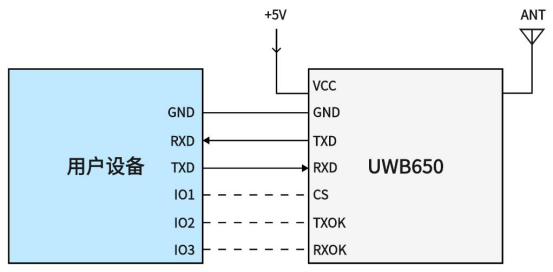
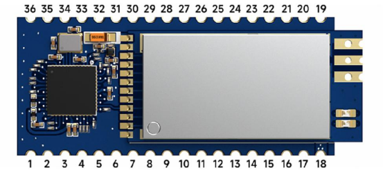
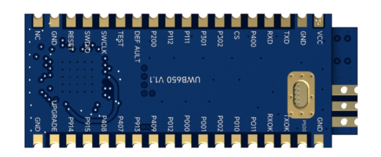
The module connects to external systems via pin interfaces, with clear pin definitions that facilitate hardware integration.


Key pins include:
Power: VCC (3.0-5.5V) and GND.
Serial Communication: RXD and TXD, used for command and data interaction with the host MCU.
Hardware Control: RESET (low-level reset), DEFAULT (long low-level hold to restore factory settings), CS (low-level to enter sleep mode), and UPGRADE (low-level to enter firmware upgrade mode).
Status Indicators: TXOK (high during data transmission), RXOK (high during data reception), and P011 (high during ranging/positioning), which provide hardware-level support for real-time status monitoring.
1.3 Key Performance Specifications and Operating Parameters
The performance parameters of the UWB650 module determine its suitability for specific applications. Detailed information on these parameters is crucial for power budgeting, power management, and performance evaluation in the early stages of system design.
The module's high transmit power of up to 27.7 dBm (~0.5W) is key to its ability to communicate over distances of more than 1 kilometer. However, this feature has different effects in different application scenarios. In open environments requiring long-range communication, high power is a significant advantage. But in close-range positioning applications (e.g., within 1 meter) that require centimeter-level accuracy, excessive power can exacerbate signal reflections, creating stronger multipath effects that may cause ranging data to drift and reduce accuracy. The module's FAQ clearly states that when used at close range, it is recommended to appropriately reduce the transmit power via the UWBRFAT+POWER command to mitigate multipath effects. This reveals a critical performance trade-off: system designers must make choices and dynamic adjustments between communication distance and near-field accuracy based on the specific needs of the application.
UWB650 Performance Parameters Table
The following table consolidates the key electrical and RF performance parameters of the UWB650 module, providing a quick reference for hardware evaluation and design.
The module uses a data frame format compliant with the IEEE 802.15.4-2020 standard for communication over the wireless link. This format includes fields such as Frame Control, Sequence Number, PAN ID, Destination Address, Source Address, Frame Payload, and Frame Check Sequence (FCS). For application layer developers, the core focus is the Frame Payload section. Data input through the serial port is encapsulated into this section for transmission, and for data received wirelessly, the module only outputs the content of the Frame Payload via the serial port. The remaining protocol fields are automatically managed by the module's firmware and cannot be modified by the user.
In-Depth Analysis of the UWB650 Module Series
 +86-755-23080616
 sales@nicerf.com
Website: https://www.nicerf.com/
Address: 309-315, 3/F, Bldg A, Hongdu business building, Zone 43, Baoan Dist, Shenzhen, China


 English


