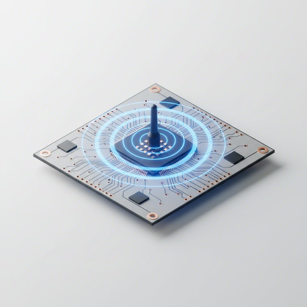
Start with the UWB fundamentals
When you sketch your first feed trace, what do you really need to know? Start by defining the signal you are radiating and how an ultra wideband radiator behaves across a very large fractional bandwidth. That context will steer every geometry and stackup choice you make.
What UWB means for antenna engineers
For antenna design, UWB means an instantaneous bandwidth > 500 MHz or a fractional bandwidth > 0.2 around the chosen center frequency.
In practice, most positioning systems today implement IEEE 802.15.4 high-rate pulse UWB with impulse radio signaling and channels in low and high bands, for example a high-band channel near 6.49 GHz with 499.2 MHz bandwidth. In the United States, unlicensed UWB spans roughly 3.1–10.6 GHz, which frames the ultra wideband frequency range many designers target for IoT and ranging. Regional rules and deployment details matter: real products have shipped on a 6.5 GHz channel with 500 MHz bandwidth under ETSI and FCC, used gated measurements due to short bursts, and required firmware adjustments or band changes for Japan where certain bands were not approved.
You might also wonder what is 5g ultra wideband. In this guide, UWB refers to IEEE 802.15.4 impulse radio used for precise ranging and localization.
Core performance pillars beyond S11
Wide fractional bandwidth changes the rules. You will notice that tiny layout or material shifts can move resonances and reshape pulses. Agree on acceptance targets before you simulate.
Impedance bandwidth that covers the chosen UWB channel set.
Radiation efficiency sufficient for your link budget and duty cycle.
Pattern stability across band and use-cases, not just at one spot frequency.
Group delay flatness with minimal ripple to avoid ringing in pulses.
Integration constraints such as ground clearance, housing proximity, and keepouts.
Regulatory awareness for regions and channels you will actually ship.
Measurable goals to log: return loss bands, group delay ripple trend, target radiation cuts.
Why time domain matters for ranging and localization
UWB uses very short pulses, often sub-nanosecond, so the antenna behaves like a very wide band-pass element. That means it can distort the waveform, introduce ringing, and shift the apparent phase center if its phase is not linear. For clean time-of-flight and angle-of-arrival, aim for non-dispersive behavior and a near-constant group delay across the operating band, otherwise centimeter-level ranging degrades even when S11 looks fine. IntechOpen.
Think system-first. Do you need omnidirectional coverage for RTLS anchors and tags, or more directive gain for longer links and multipath control? Is compact form factor more important than efficiency? Lock those answers now, and the geometry, stackup, and test plan in the next sections will follow naturally.
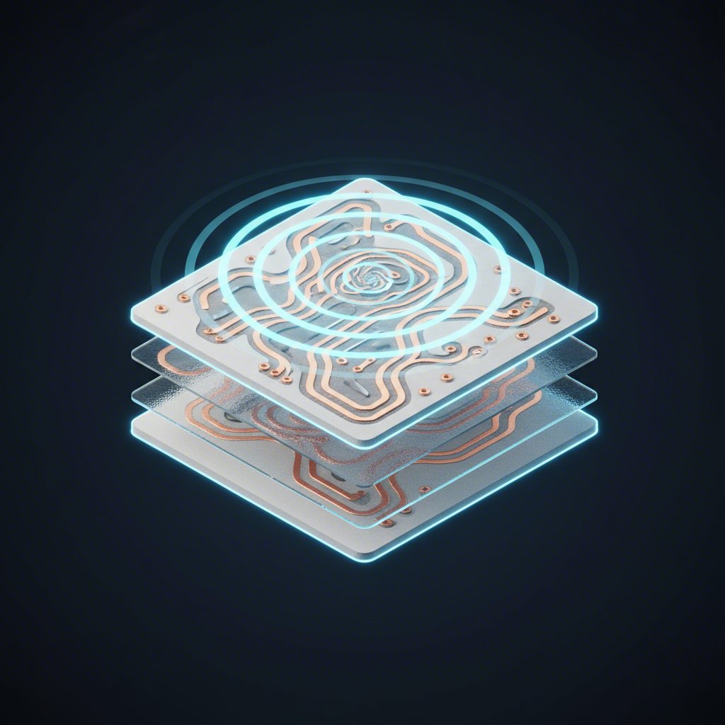
Choose substrates and stackups wisely
Why do two boards with the same CAD look different on the bench? In UWB, the stack-up often decides whether your wideband antenna preserves frequency bandwidth and pulse shape, or turns your waveform into ringing and loss.
Substrate and stack-up decisions that widen bandwidth
Substrate Dk, loss tangent, thickness, and copper all shape impedance, efficiency, and dispersion. FR-4 is economical but its dielectric constant varies with frequency, temperature, and humidity, and its loss tangent rises at higher GHz, while RF laminates hold Dk tightly and run with far lower loss. Thin-film stacks using polyimide with a high-Dk adhesive can miniaturize radiators while maintaining good time-domain behavior in the UWB high band.
Option | Dk and loss | Bandwidth and efficiency impact | Fabrication and tolerance sensitivity | Notes for UWB |
FR-4 laminate | Dk ~4.2–4.7 at 1 GHz with variability; loss tangent ~0.02 at 1 GHz, higher at 10 GHz | Higher loss can reduce efficiency near the top of antenna wideband; Dk drift can detune | Low cost, widely available, shorter lead times | Practical up to ~6–10 GHz for non-critical use; watch dispersion and repeatability |
Low-loss RF laminate | Tight Dk control and low loss tangent down to ~0.0012 at 10 GHz in some families | Supports wider usable frequency bandwidth and cleaner phase | Higher cost, specialized handling, potentially longer lead times | Better for tight impedance and low-loss UWB designs |
Thin-film PI + high-Dk adhesive | Example PI Dk ~3.3, adhesive Dk ~6, thin copper and films | High-Dk layer enables size reduction with trade-offs in bandwidth | Very thin stack-ups are sensitive to bonding and connector effects | Measured high-band UWB antennas showed wide S11 bandwidth and stable group delay |
Finish and copper uniformity | Process-dependent | Inconsistent plating or roughness can perturb impedance | Keep finish type consistent across builds | Confirm finish early to reduce unit-to-unit variability |
Manufacturing tolerances that detune UWB antennas
Small physical errors produce large fractional shifts over an antenna wideband span.
You will notice that tiny changes in dielectric thickness, copper thickness, or soldermask creep near the feed can move resonances and ripple group delay. Protect the radiator with keepouts and use soldermask pullback around the feed to reduce capacitive loading. Maintain ground clearance under and around the radiator, and use dense via fences to keep the launch well behaved.
Ask the fabricator for full tolerance stacks on dielectric thickness and Dk.
Run worst-case sweeps of substrate thickness and permittivity within vendor limits.
Specify controlled copper thickness and confirm plating targets.
Panelize consistently to avoid edge effects on outer coupons.
- DFM checklist to confirm: trace widths, copper thickness, dielectric thickness, mask registration, finish type, via drill and plating, panelization method.
Connector and launch effects at the board edge
At UWB, the board-edge launch can dominate what you measure. In a thin, compact UWB monopole, the board-edge SMA and its widened ground significantly altered results, so a one-port de-embedding workflow was used to remove the connector from S11. Even then, cable loss and soldering introduced small discrepancies between simulation and measurement, while the antenna still delivered a measured S11 bandwidth spanning about 5–10.8 GHz with stable group delay in the 6–9 GHz high band, underscoring the need for careful fixtures and de-embedding. MDPI Electronics.
Locking in a robust stack-up makes it much easier to choose the right radiator family next, where topology sets most of your pattern and size trade-offs.
Compare UWB antenna topologies for omnidirectional and directional needs
Choosing a radiator feels like guesswork? Start by matching the physics of each ultra wideband antenna type to your system goals. If you want reliable ranging, prioritize stable patterns and clean time response. If you need distance, consider directional gain and physical aperture.
Choosing the right topology for your constraints
Printed monopoles are go-to for compact uwb antenna designs because they can span very wide bands with near-omnidirectional behavior, while tapered slot or quasi-Yagi structures deliver higher directivity for longer links. Published prototypes show printed monopoles covering about 1.6–12.4 GHz with nearly omnidirectional patterns, and a flared quasi-Yagi achieving 3.06–12.37 GHz with about 10 dBi peak gain and high efficiency, illustrating the breadth of options ResearchGate. Use omnidirectional antennas for tags and anchors that must hear from any angle, and choose directional tapered slots to push range or reduce multipath in cluttered venues.
Topology selection sets 80% of your integration burden; matching can only polish, not reinvent, pattern physics.
Topology | Relative bandwidth | Efficiency | Omnidirectional behavior | Size | Integration complexity |
Printed monopole | High | Medium–High | High | Medium | Low–Medium |
Planar inverted-F variants | Medium | Medium | Medium | Small | Medium |
Slots and rings | High | Medium–High | Medium–High | Medium | Medium |
Tapered slot or Vivaldi | High | High | Low | Large | High |
Patch with slots/notches | Medium | Medium–High | Medium | Medium | Medium |
Beveled or compact shapes | Medium–High | Medium | Medium–High | Small–Medium | Medium |
Pattern stability and body loading effects
Hands, batteries, and human tissue can detune antennas and reduce efficiency. When a radiator is placed on lossy human phantoms, measured impedance increased by roughly 17–20%, radiated power dropped about 9–11%, and efficiency and gain decreased accordingly, underscoring the need for margin and careful placement PMC. For wearable or handheld products, reserve extra ground clearance, avoid placing metal near the radiating edges, and validate patterns with and without the enclosure.
Space-limited products and ground clearance rules
In tight layouts, prioritize ground-dependent radiators that tolerate smaller boards, but still enforce keepouts, launch control, and casing materials with low permittivity and loss. Finalize placement early, keep metal away from the radiator, and tune only after the mechanicals settle.
Printed monopole: preserve partial-ground cutouts, keep the feed region free of soldermask creep, and test with the final bezel installed.
Planar inverted-F: maintain stable shorting path and consistent reference ground, and watch for body-proximity detuning.
Slots and rings: keep uniform ground around the slot, control CPW or microstrip clearances, and avoid metal labels over the aperture.
Tapered slot or Vivaldi: provide open aperture space and absorber-free line of sight; route cables away from the flare.
Patch with slots/notches: verify that notches do not introduce unwanted group delay ripple across the UWB band.
Next, we will turn these comparisons into a reproducible printed monopole workflow you can run from first sketch to chamber.
Step by step UWB printed monopole design
Sounds complex? Use a repeatable flow and let data steer the edits. This approach works well for compact uwb antennas that must behave like a wide bandwidth antenna for precise ranging.
Reference geometry and first-order sizing
Start simple. A printed monopole with a partial ground and CPW or microstrip feed is a proven wide band antenna building block. Ground size sets the lower edge and pattern balance, so plan early sweeps of the board ground dimensions before you chase radiator details. Simulations and measurements have shown that shrinking the ground can raise the lower edge frequency and narrow the impedance bandwidth while patterns remain broadly omnidirectional, which is critical context for layout keepouts ISAP 2007.
Define bands of interest. Note target channel set, pattern goals, and acceptable group delay ripple across the operating span.
Select substrate and thickness. As a validated reference, a CPW fed UWB monopole on Rogers RT5880 with 1.575 mm thickness and Dk 2.2 has been used successfully for wideband studies and time domain analysis.
Draft radiator and ground cutout. Reserve a clean keepout under the radiator. Plan to sweep ground size because it shifts the lower edge and affects omnidirectionality, as observed in UWB monopole studies.
Add feed and launch. Use a controlled CPW or microstrip feed. Set open boundaries in the EM tool with an airbox far from the geometry to approximate free space. Calibrate and, if possible, de-embed connectors so the feed does not mask antenna behavior.
Run EM sweeps on radiator length, bevels or notches, and ground slots. Use adaptive meshing where practical and check convergence by refining the mesh and re-running a few points.
Evaluate S11 and group delay. Convert S-parameters to group delay by taking the negative slope of the transmission phase versus frequency. Flat group delay indicates cleaner pulse fidelity.
Export to PCB with manufacturing constraints applied. Add soldermask pullback at the feed, maintain ground clearance, and place via fences consistently to stabilize the launch.
Prepare test coupons. Include bare antenna coupons and feed-through standards to verify calibration, connector quality, and de-embedding workflows.
Parametric sweeps to center target bands
Think coarse to fine. First, sweep radiator height and width together to slide the band. Next, trim edges with bevels or small notches to smooth return loss. Then, adjust the ground window and any slots to improve bandwidth and pattern stability. Recheck that S11, S21 phase, and group delay remain smooth across your channels rather than at one spot frequency. If orientation matters in your product, include off-broadside pattern and phase checks during sweeps so you do not trade bandwidth for dispersive behavior IEEE TAP.
From EM model to PCB with minimal drift
Bridging sim to bench is where many wide designs drift. Match the as-built stack-up and finish in your EM model. Keep the connector, pad, and launch geometry identical between CAD and the chamber. Use TOSM or equivalent calibration to move the reference plane to the antenna feed and de-embed fixtures where tools allow. Then overlay multiple units to confirm repeatability and tolerance sensitivity.
Feed-region copper and the nearby ground or via fences often dominate resonance more than fine radiator art in a wide band antenna.
Sanity checks before fab
Confirm airbox and boundary settings are far enough to avoid reflection coupling.
Verify mesh convergence at several frequencies across the band.
Export Gerbers with mask pullback around the feed gap and controlled copper thickness notes.
Include a ground-only coupon and a thru line for de-embedding practice.
Plan to compute group delay and inspect any ringing in time-domain transforms after first articles.
With geometry locked, the next step is to measure time domain behavior and group delay to ensure the antenna preserves pulse fidelity for ranging.
Time domain performance and measurement
You locked the geometry. Now how do you know your pulses stay clean for ranging and AoA? Time-domain checks tell you if the radiator preserves waveform shape across the ultra wideband frequency span.
Group delay ripple targets for clean ranging
For precise TDoA and uwb tracking, focus on three ideas. Group delay flatness means the antenna phase is nearly linear with frequency. Pulse fidelity describes how closely the received pulse matches the transmitted template. Ringing is the unwanted energy before or after the main lobe.
As a practical rule, keep group delay variation within about 1 ns across the band and the antenna transfer function variation within 10 dB.
These limits reflect published time-domain evaluations where even well matched antennas broadened pulses when higher order modes shifted the phase center with frequency, degrading ranging despite good S11 IntechOpen.
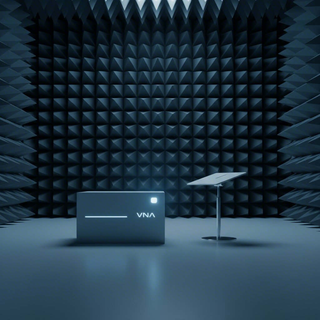
From S-parameters to time-domain insight
Sounds complex? You can get there with a VNA. Measure S11 and, when possible, S21 between two antennas. Apply a time-domain transform to reveal the impulse response, then use windowing and gating to separate fixtures and launches from the radiator.
Set a wide frequency span and enough points to improve time resolution and time range.
Choose bandpass mode for band-limited DUTs, or lowpass when DC behavior matters.
Apply windowing to trade off main-lobe width and sidelobes, then enable time gating to remove fixture echoes and re-project the cleaned result to frequency.
Capture impulse response, compute group delay from the phase slope, and note any pre or post ringing tied to geometric features.
Document settings so later runs are comparable.
A VNA workflow with time-domain transforms, windowing, and gating is well established for antennas and interconnects.
Interpreting distortion that hurts uwb tracking
You will notice that clean antennas show a single narrow main lobe with small FWHM and fast decay. Excess ripple in group delay or strong sidelobes signals multi-mode behavior that can bias AoA or stretch time-of-flight in uwb applications.
Practical test setups and de-embedding tips
Measure S21 in a simple LOS path at consistent distance and polarization.
Calibrate at the connector plane and de-embed launches where possible.
Use time gating to remove cable and fixture reflections before assessing the antenna.
Overlay multiple DUTs to spot unit-to-unit variation and tolerance sensitivity.
Correlate time-domain anomalies back to feed copper, ground windows, or enclosure metal.
Bottom line, an antenna can meet return loss yet still fail ranging if pulse distortion is high across the ultra wideband frequency span. Verify time-domain metrics first, then move to wideband matching and RF integration to preserve them.
Wideband matching and RF integration
Chasing a few more dB of return loss without wrecking pulse fidelity? The right approach keeps bandwidth wide and group delay smooth so ranging and AoA stay accurate.
When to match and when to re-shape the radiator
Start with the bare antenna. If its Smith chart locus already skirts 50 Ω across much of the band, favor radiator and ground tweaks over complex matching. Remember, a simple L-section gives a conjugate match at one frequency, while true broadband matching needs a bandpass-style network optimized across a span MathWorks. Keep networks minimal to avoid resonant traps and group delay ripple. Also, account for SMD parasitics and tolerance—uncompensated values can shift the response by hundreds of megahertz, and yield improves dramatically when you tighten tolerances around the GHz range. This section focuses on impulse UWB antenna matching rather than 5g uwb or what is ultra wide band 5g labels, and should not be conflated with any frequency for bluetooth considerations.
Smith chart workflow for wideband antennas
Measure de-embedded antenna impedance across your operational UWB span. Plot the trajectory on a Smith chart.
Decide if a single series or shunt element broadens the usable band. If not, consider a modest bandpass-style network and optimize average reflection over frequency rather than a single-notch target.
Model real components: include ESR, ESL, SRF, and package effects. Parasitics can move the match by hundreds of megahertz, and using 5% tolerance parts around a 2.4–2.6 GHz target band achieved about 99.3% yield for S11 ≤ −10 dB, versus 81.9% with 10% tolerance.
Keep interconnects short and avoid stubs. For 0402 networks, ~0.5 mm links between pads have minimal impact up to several GHz when laid out carefully.
Validate in both domains: check S11 flatness and compute time-domain response and group delay to confirm the match did not add ringing.
Layout rules that keep the match transparent
Use grounded coplanar waveguide, with a continuous backside ground and symmetric launches. Add via fences tied to the ground planes; space vias no more than λ/10 at the highest frequency and place the fence roughly one to three gap-widths from the signal edge for isolation without overloading the line.
Do | Don’t |
Use low-tolerance parts and verify SRF is above your band | Rely on high-Q elements that create narrow traps and ripple |
Place elements close together with short, symmetric routes | Add long stubs, meanders, or asymmetry near the feed |
De-embed launches and check group delay after any change | Judge success by S11 alone without time-domain checks |
Match gently. Most wideband wins come from radiator and ground tuning, with a light-touch network to smooth the last edges. Preserving that phase linearity sets up your array calibration and AoA processing to work cleanly in the next stage.
Array calibration for precise AoA in UWB array design
Want sub degree angle of arrival UWB estimates that hold up outside the lab? Start by pairing good geometry with a repeatable aoa calibration flow. You will notice that symmetry, spacing, and phase control do most of the heavy lifting before any DSP touches the data.
Array geometry that preserves omnidirectional cues
Element spacing sets your unambiguous phase window. As a practical target, place elements near 0.45 lambda at the channel center to avoid phase wrapping yet keep resolution high. For dual band arrays, size spacing for the higher band so the lower band remains within the safe phase range. Keep group delay variation low across the useful aperture and band, and plan for front back ambiguity. Monopoles need cues from IMU data, directional patterns, or a third element to resolve it. Maintain 50 ohm feeds and consistent routing so your calibration only removes small residual errors.
Isolation and mutual coupling mitigation
Coupling blurs phase. Aim for at least 25 dB isolation between elements and use ground slots, fences, or absorbing structures where layout allows. Prefer on board feeds with short, equal length lines. Micro coax can add bend sensitive phase shifts and force per unit calibration. For uwb array design, treat the enclosure as part of the array. Make the environment symmetric and keep large metal, batteries, and display frames balanced around the array center.
Preserve symmetric ground clearances and bezel distances across elements.
Keep feed lengths consistent and avoid vias in RF paths when possible.
Route cables away from flares or radiators and mirror their paths left to right.
Use dense via fences to confine CPWG fields and reduce cross coupling.
Place nearby metals either far away or symmetrically to simplify DSP corrections.
In post processing, wideband mutual coupling mitigation can leverage element pattern reconstruction to transform embedded patterns toward isolated ones and decouple received signals across subbands, which is effective for planar arrays as well as wire elements International Journal of Antennas and Propagation.
Repeatable calibration for field deployment
Small phase errors across wide bands accumulate into large AoA bias.
Lab reference. Use a known UWB source and a turntable to sweep azimuth. Record per element phase and amplitude vs angle at each operating channel.
Per channel equalization. Compute amplitude and phase offsets at 0 degree and across the band. Store offsets so PDoA is centered and band to band drift is removed.
Element pattern characterization. Log embedded element patterns with the final enclosure installed. Gate out fixtures and verify group delay flatness across the operational span.
Mutual coupling correction. Build a wideband compensation matrix from measured patterns or EM models and apply it in DSP during PDoA estimation.
Periodic in field check. Use a portable reference beacon at a known bearing to refresh offsets and confirm array health after shocks or service.
Robust antenna delay and bias calibration materially improves localization; one study reported an average 46 percent improvement in accuracy when calibrated and when measurement uncertainty was modeled vs received power arXiv. If your calibrated array still shows bias or jumpy angles, move on to the troubleshooting and validation workflow next.
Troubleshooting and validation workflow
When your prototype misses range or AoA targets, where do you start? Use this field-proven antenna troubleshooting flow to isolate S11 anomalies, radiation pattern distortion, gain shortfalls, and unit-to-unit drift during uwb antenna testing.
Systematic S11 triage before geometry changes
Sounds obvious, but verify the measurement first. Bad references hide real issues and waste spins.
Do s11 troubleshooting with a fresh calibration at the antenna feed plane, not the VNA port. De-embed launches and fixtures where possible.
Sweep a span that covers all intended UWB channels. Use enough points to improve time resolution when you transform to time domain.
Apply time gating and windowing to remove fixture echoes before judging the radiator. VNAs support bandpass transforms, gating, and window trade-offs that reveal discontinuities clearly.
Pattern and efficiency checks that isolate root causes
If S11 looks fine but links are short or angles bias, look at patterns and losses.
Test in free space first, then add the enclosure piece by piece. Nearby metal can shift sidelobes, fill nulls, and even add a few dB in unpredictable directions in the near field, so do not rely on nominal nulls when hardware is close WIT Press.
Recheck keep-outs around the radiator and battery. Maintaining separation, for example about 20 mm from a battery, reduces detuning risk and preserves radiation efficiency.
Manufacturing defects and how to spot them fast
Inspect the launch: pad length, solder fillets, mask creep, and ground gaps dominate wideband behavior.
Microscope or X-ray vias for opens or thin plating. Compare multiple units to quantify process spread.
Confirm the as-built stack-up and finish match the EM model.
Verify calibration and de-embedding.
Inspect connector and launch solder.
Compare to a bare test coupon.
Sweep enclosure proximity and orientations.
X-ray or microscope for vias and copper opens.
Re-measure with cables repositioned and strain-relieved.
Run time-domain transform to locate discontinuities and apply gating.
Update EM with the as-built stack-up and refit parameters.
Symptom | Likely cause | Quick fix |
S11 band shifted high | Thinner dielectric, longer launch pad, mask loading | De-embed, trim feed copper, pull back soldermask, refit Dk in EM |
Good S11, poor range | Lossy path or dispersive match adding group delay ripple | Simplify matching, check time-domain response, reduce high-Q parts |
Radiation pattern distortion in enclosure | Nearby metal or battery coupling | Increase keep-out, add absorber judiciously, validate patterns with enclosure installed |
Low gain vs model | Connector loss, rough copper, mis-cal | Recalibrate, gate out fixtures, confirm finish and copper thickness |
Unit-to-unit variability | Mask registration, via plating spread | Tighten fab tolerances, overlay multiple DUTs, tune to median |
Repeatable fixtures and consistent cable dressing are as important as the antenna itself.
Set acceptance up front. Define pass bands for return loss across your UWB channels, pattern uniformity windows in the key cuts, and limits on group delay ripple and time-domain ringing after gating. For products with metal nearby, use a protective envelope for off-axis gain rather than trusting ideal nulls due to near-field uncertainty noted above. Once you pass this checklist, move to module-aware verification to confirm performance at real power levels and waveforms.
Module-aware UWB antenna integration
Bringing your design onto real hardware now? This is where uwb module integration turns a good radiator into a reliable product. Your antenna must preserve pulse fidelity, support the uwb link budget, and stay compliant at the module’s power levels and bands.
As a concrete reference point, the NiceRF UWB650Pro is built on the Qorvo DW3000, supports IEEE 802.15.4-2020 on Channel 5 at 6489.6 MHz with 499.2 MHz bandwidth, integrates an RF amplifier and MCU with UART control, offers up to 0.5 W or 27 dBm transmit power, advertises 1 km communication distance, and specifies ranging accuracy better than ±10 cm with sleep current below 100 μA. These capabilities set practical constraints for antenna selection, matching, and placement in your system. NiceRF UWB650Pro.
Antenna integration checks for long-range UWB
Impedance and phase. Target S11 below −10 dB within the desired 500 MHz band, and keep group delay variation low to protect pulse shape. Qorvo recommends minimizing group delay variation to under about 100 ps within a 500 MHz band and using 50 Ω controlled-impedance feed lines with short, similar lengths. Avoid vias in the RF path, prefer CPW with ground and via fences, and beware micro coax because bending and length tolerances add phase shift per millimeter, which stresses AoA and ranging accuracy.
Coexistence. If you add band-pass or notch filters for nearby services, budget their insertion loss and group delay. Filters can introduce phase nonlinearity that stacks with the antenna’s dispersion.
DW3000 antenna path. Keep the dw3000 antenna feeds short, symmetric, and isolated from noisy clocks and high-speed digital lines.
Performance modes. Validate at the module’s supported data rates and power settings so pattern stability and group delay hold across operational modes.
Antenna verification steps tied to module bring-up
Configure the module on Channel 5 and sweep both 850 kbps and 6.8 Mbps modes to capture representative spectra. NiceRF UWB650Pro.
Measure S11 at the antenna feed, de-embedding the launch. Gate time-domain responses to isolate radiator behavior and compute group delay across the 500 MHz band.
Over-the-air S21. In a controlled LOS setup, collect S21 versus frequency between two units to verify pulse fidelity and range trends consistent with your uwb link budget.
Pattern with the real enclosure. Mount the final housing and log embedded patterns at representative power levels to confirm off-axis uniformity and AoA bias control.
Regional readiness. If you need EU, US, or Japan, verify gating, duty-cycle behavior, and spectral shaping. Case studies show systems meeting ETSI and FCC on 6.5 GHz with 500 MHz bandwidth, using gated measurements and, when needed, a notch below 7.125 GHz to coexist with 6 GHz Wi-Fi. Japan often requires firmware or band adjustments.
Power handling and EIRP compliance
Imagine turning on a 27 dBm profile and seeing pattern or group delay shift. Higher drive can expose weak spots in matching, feed layout, or filters. Evaluate linearity and thermal behavior at maximum allowed settings before you rely on long-range profiles.
Integrated PAs and long-range modes tighten requirements on antenna efficiency, linearity, and group delay.
Check EIRP compliance by band and region when using high transmit power. Use gated measurements and low-duty-cycle profiles where required by local rules, and confirm that any filters used for coexistence do not push group delay beyond your ranging budget.
Budget dispersion. A discrete filter can add tens of picoseconds of group delay variation across part of the band, which stacks with antenna dispersion; keep the combined variation inside your timing error budget.
Mechanical placement that protects pattern integrity
Unobstructed view. For on-device arrays or single elements, keep an open sector in front of the antenna and avoid covers that load the radiator. Symmetry reduces AoA bias.
Ground and keepouts. Reserve ground clearance around the feed and radiator edges, keep metal batteries and brackets at consistent distances, and route cables away from the radiating aperture.
Launch discipline. Use CPWG with dense via fences, avoid layer transitions in the RF path, and keep feeds short to maintain pattern stability across the band.
Document antenna placement uwb constraints in the mechanical spec so late changes do not detune the design.
Once the module-level tests pass at real power and waveforms, lock your settings and move to the final checklist and tools to speed repeatable validation across EVT and beyond.
Final UWB design checklist and recommended tools
Ready to leave the lab and scale with confidence? Use this practical uwb design checklist to keep pulse fidelity, patterns, and yield on track from concept to production.
Design and verification checklist
Requirements. Lock channels, link budget, target patterns, and acceptable group delay ripple. Published UWB prototypes have demonstrated group delay under about 1 ns across band, a useful benchmark when you set limits.
Topology and placement. Pick a radiator family that fits space and pattern needs, then reserve ground clearances and keepouts in CAD early.
EM simulation workflow. Set up parametric sweeps, adaptive meshing, and de-embedding. Choose solvers and flows in CST, HFSS, or ADS based on your model scale and goals.
RF PCB DFM. Specify stack-up, copper thickness, finish, mask pullback near feeds, via fences, and panelization. Confirm tolerance stacks with your vendor.
Matching and time domain. Prefer minimal networks. Validate S11 and compute group delay and impulse response after any change.
Enclosure effects. Measure patterns and efficiency with the final housing installed. Compare to bare coupons.
Module bring-up. Use the NiceRF UWB650Pro as a reference platform to validate antenna KPIs against ranging accuracy and link margin in field trials. NiceRF UWB650Pro.
Arrays and AoA. Target strong isolation and pattern symmetry. In UWB MIMO literature, isolation above 20 dB is commonly cited as high, guiding array spacing and decoupling choices SSRG review.
Tools and templates that speed iteration
- Antenna validation tools. VNA with time-domain transform, gating, and de-embedding. Anechoic chamber with turntable for patterns.
- EM tools. CST, HFSS, or ADS for fast parametrics and optimization within a documented em simulation workflow.
- RF PCB DFM templates. Stack-up and tolerance forms, mask and finish checklists, and as-built capture sheets.
- Data packages. Versioned S-parameters, group delay plots, radiation patterns, and correlation notes across builds.
Validate with as-built stack-up and real waveforms before EVT exit.
From prototype to scalable manufacturing
Create a golden unit and guardband limits from chamber data.
Archive test artifacts for every spin:
S-parameters and de-embedding settings
Group delay and impulse response plots
Radiation patterns with and without enclosure
As-built fab notes, stack-up, finish, copper thickness, mask registration
Array calibration files and offsets if applicable
Lock rf pcb dfm rules into the release package and track SPC on dielectric thickness, copper, and mask.
Run pilot field tests on the UWB650Pro platform to link antenna KPIs to ranging error and link margin before scaling.
Follow this checklist, and you will ship antennas that hold pattern, preserve pulses, and scale cleanly from bench to field.
UWB antenna design considerations: FAQs
1. What frequency range does UWB cover for antenna design?
For antenna work, UWB generally means at least 500 MHz of instantaneous bandwidth or a fractional bandwidth above 0.2. In the US, unlicensed UWB spans roughly 3.1–10.6 GHz, and many systems operate a high‑band channel around 6.49 GHz with about 499.2 MHz bandwidth. Real deployments often focus on a 6.5 GHz channel with a 500 MHz span, but regional rules vary. Treat compliance as a design input and confirm your final channel plan early.
2. Why does group delay flatness matter for UWB ranging and AoA?
UWB uses very short pulses, so the antenna’s phase linearity directly affects pulse shape and timing. Excess group‑delay ripple introduces ringing and shifts the apparent phase center, causing range and angle bias even when S11 looks acceptable. As practical guidance from the article, keep total variation around 1 ns across band for clean ranging, and note that vendor guidance targets about 100 ps within a 500 MHz band for tighter AoA performance. Always validate in both frequency and time domains.
3. Which UWB antenna topologies are best for ranging vs long‑range links?
For tags and anchors that need uniform coverage, printed monopoles are a strong choice thanks to wide bandwidth and near‑omnidirectional patterns. When you need more distance or want to mitigate multipath, tapered slot or Vivaldi‑style antennas provide useful directivity at the cost of size and integration complexity. Slots, rings, and notched patches can balance size and bandwidth, while PIFA variants help when space is tight but may demand more careful housing integration.
4. How do PCB materials and tolerances impact UWB antenna performance?
Dielectric constant, loss tangent, and thickness strongly influence impedance, bandwidth, and dispersion. FR‑4’s variability can detune and add loss at higher GHz, while low‑loss RF laminates hold Dk tightly and improve efficiency. Small physical errors in copper thickness, soldermask creep, and launch geometry produce large fractional shifts across a wideband span. Use soldermask pullback near the feed, maintain ground clearance, control copper and finish, and de‑embed the board‑edge launch during measurement.
5. How should I validate a UWB antenna with a DW3000‑based NiceRF UWB650Pro module?
Verify at the module’s operating band and power levels. For UWB650Pro, that includes the high‑band Channel 5 around 6.4896 GHz with roughly 499.2 MHz bandwidth and up to 0.5 W transmit power. Measure S11 at the antenna feed with de‑embedding, compute group delay across the band, run over‑the‑air S21 in a controlled line‑of‑sight setup, and confirm embedded patterns in the final enclosure. Check EIRP compliance by region and ensure time‑domain fidelity aligns with the module’s ranging targets and long‑range modes.
 English


 +86-755-23080616
 sales@nicerf.com

