Walkie-Talkie Module TDD Noise: Principles, Quick Fixes, and System-Level Solutions
Nov . 2025
Introduction

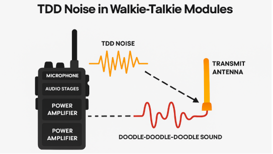
Our NiceRF engineers found that debugging led them to listen to the "doodle-doodle-doodle" TDD noise repeatedly while developing DMR digital walkie-talkie modules under transmit mode. I've seen many teams think that the audio chip is the problem. However, it's not a chip problem but the current pulse generated during Time Division Duplex (TDD) transitions while in transmit-receive mode that sort-of "injects into" the audio path through power/ground loops, PCB layout coupling, and microphone bias circuits.
In this article, I will share the learning from practice: why noise is present, how to quickly find it, how to get rid of it step by step—i.e., from "insert a suitable power inductor" to "four-layer board and anti-interference layout"—all while covering the topics of component selection, waveform analysis, and decision tree.

What is TDD Noise? (Phenomenon and Principle)
What we've found is that many engineers who are new to the industry don't understand TDD noise.
1.1 Phenomenon and Root Cause
Phenomenon: During PTT press of the Push-to-Talk (PTT) button/during TX time slot, a low "doodle" sound with odd harmonics (10s-100s Hz) in ranges from 16-20Hz is heard at speaker or headset, like "motor/machine gun".
Cause (Layman Terms): In TDD Mode of operation, the Power Amplifier (PA) is turned ON and OFF intermittently based on time-slot. This "pulsation" gets out via power/ground/coupling paths into the audio section, in which it is "demodulated" as a low-frequency envelope by/within this audio stage and thus becomes audible.
1.2 Engineering Summary: The Three Paths of TDD Noise Propagation
Our NiceRF design experiences have proved that TDD noise can be abstracted to three common kinds of propagation paths in engineering:
Power Supply Crosstalk (PI Issue): TDD pulsing induces ripple/voltage drop on the power/ground, and "jitters" audio reference.
Layout Coupling (EMI Problem): The high current loop of RF/PA is nearby with the lines of MIC/Audio/Control, which leads to capacitive/inductive/common impedance coupling.
Not Enough Filtering: The separation of the microphone bias and Clean Power (3.3V) is too weak, or LDO's Power Supply Rejection Ratio (PSRR) is too low.
Tip: A TDD frame is usually 60 ms and has a fundamental frequency of f0 = 1/60ms = 16.7 Hz; what you witness as the "nice little teeth" in the spectrum are its harmonic comb lines.
Three "Quick" Noise Canceling and Noise Suppression Routes - Instant Results!
Of these, I suggest three ways for initial import or during prototyping; they do not require significant reworking and can validate the result very fast:
2.1 Type A Route | Power Input: "L + C" Isolation (Recommended)
Method: Put a series 15 µH, ≥1.3 A power inductor at the module's input, and add 100 µF (low ESR) + 10 µF + 100nF near-end decoupling.
Function: Provides a low-pass filter to trap TDD low frequency envelope & switching spikes on the "dirty side".
2.2 Option B | "Clean" 3.3V for Audio/Baseband (High PSRR LDO)
Method: Use low-noise LDO with high PSRR (commercially available XC6228D33 or similar) from 10 Hz to 1 MHz (>70 dB) to power supply for baseband/audio/MIC bias.
Purpose: Minimizes input ripple and provides isolation from the "dirty power supply".
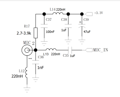
2.3 Route C | Microphone Bias "Three-Stage" Filtering + Ground Guarding
Method: Implement 3rd order filter for the MIC Vbias (47µF + 10µF + 2.2µF Tantalum or stable dielectric) and surround MIC_Voltage with continuous solid ground copper (Ground Guarding/Via Fence).
Operation: Clips the envelope at the bias end, ensuring only sound is "heard" by the microphone, not 30V!
[Contact us now] Get in touch with our engineers to learn more about optimizing noise for various PCB designs!
Engineering Solutions (Power Integrity/PCB/Components) at the System Level
The NiceRF practices indicate that full TDD noise cannot be completely wiped out, and it requires solving PI problems and PCB layout at the system level.
3.1 Need for Power Integrity (PI) Design
Target Impedance Approach: Ztarget = ΔV/ΔI. For instance, if the transmit step ΔI = 0.5A and an allowable ΔV = 50mV, then Ztarget ≤ 0.1 Ω.
Decoupling Layering:
100 nF (High Frequency) placed close to pin
10 µF (Mid Frequency) in near area
100 µF (Low Frequency) at input
Inductor Selection: Isat ≥ 1.5 × Ipeak, DCR < 50 mΩ, isolation > 20 dB.

2025 TDD Noise FAQ
Q1: Is addition of a single power inductor sufficient?
A: It tends to be a good fit when "input ripple is the key issue" and can be quickly checked. If it's not only the MIC bias/layout coupling that becomes the issue, then High PSRR LDO + Three-Stage Bias Filtering + Ground Guarding should be applied. Our cross-project validation implies that a system-level approach can more effectively suppress the noise at the root.
Q2: Why has the noise of the device increased when I put a very large capacitor?
A: It probably added new resonant/return paths or caused a mismatch in LDO stability. Our NiceRF practice is to comply with the capacitance/ESR window available in the datasheet, place capacitors close to the source, and verify the loop area to avoid creating new noise sources.
Q3: Why do you hear a "louder noise" when two modules come close?
A: This is the "beat frequency" effect, when multiple modules operate wirelessly in asynchronous TDD mode, allowing noise to stack up. The solution might be to experiment with TDD timing synchronization through the host controller, or to improve physical isolation/shielding between modules.
Welcome to Technical Communication
We welcome further technical discussions and can provide comprehensive TDD noise system optimization schemes tailored to your specific requirements.
Technical Support:
Email: sales@nicerf.com (Pre-sales/After-sales)
Website: www.nicerf.com (Products/Documentation/Case Studies)
 +86-755-23080616
 sales@nicerf.com
Website: https://www.nicerf.com/
Address: 309-315, 3/F, Bldg A, Hongdu business building, Zone 43, Baoan Dist, Shenzhen, China


 English


