

 English


LoRa1268 : SX1268 160mW Wireless Module With ESD protection
Certification: Others
Modulation: LoRa
Chip: SX1268
Interface: SPI
Output Power: 160mW
Frequency: 433MHz/470MHz
Size (mm):16*16


The LoRa2012 module is based on Semtech's LR2012 chip, which integrates the fourth-generation LoRa® IP core and supports sub-GHz and ISM frequency bands. It is fully backward compatible with previous LoRa devices, ensuring seamless interoperability with LoRaWAN® networks.
The LoRa2012 is manufactured and tested using a strictly lead-free process and complies with the RoHS and REACH environmental standards.
Parameters | Test condition | Min. | Typ. | Max | Unit |
Voltage range | 1.8 | 3.3 | 3.6 | V | |
Operating Temperature | -40 | 25 | 85 | ℃ | |
Maximum Input Signal | 10 | dBm | |||
Current Consumption | |||||
Transmit Current | @433MHz | < 110 | mA | ||
@868/915MHz | < 120 | mA | |||
Receive Current | @3.3V,@DCDC,Sub-GHz | < 6 | mA | ||
@3.3V,@LDO,Sub-GHz | < 9.3 | mA | |||
Sleep Current | @3.3V | ≤2 | uA | ||
RF Parameters | |||||
Frequency Range | @433MHz | 400 | 460 | MHz | |
@470MHz | 470 | 510 | MHz | ||
@868MHz | 850 | 890 | MHz | ||
@915MHz | 900 | 940 | MHz | ||
Transmit Power | @Sub-GHz | 19 | 21 | 22 | dBm |
Receive Sensitivity | BW=62.5KHz, SF=12 @Sub-GHz | -143 | dBm | ||
BW=125KHz, SF=10 @Sub-GHz | -136 | dBm | |||
Frequency Error | @Crystal | 10 | ppm | ||
@TCXO | 0.5 | ppm | |||
Modulation Rate (@sub-GHz) | @LoRa | 0.0458 | 125 | Kbps | |
@FRLC | 260 | 2600 | Kbps | ||
@FSK,@863-2.5GHz | 0.5 | 2000 | Kbps | ||
Modulation Rate (@sub-GHz) | @LoRa | 0.0458 | 125 | Kbps | |
@FSK,@433MHz-960MHz | 0.476 | 101.5 | Kbps | ||
Sub-GHz Bands: 433/470/868/915MHz (Customizable range: 150~960 MHz)
Transmission distance: >5000 meters at sub-GHz in open area
Sub-GHz reception sensitivity: up to -143dBm@BW=62.5 KHz, SF=12
Built-in electrostatic protection circuit
LoRa: modulation rate up to 125 kbps
4th Generation LoRa IP technology
Simultaneous reception with multiple Spreading Factors (SF)
Enhanced CAD (Channel Activity Detection)
Higher frequency offset tolerance (for harsh RF environments).
Supports multiple communication protocols
Transmit power is adjustable, up to 22dBm
Sleep current ≤ 2µA
Receive current < 7mA
Drones/UAV Applications
Smart home/Smart agriculture
Remote irrigation
Industrial manufacturing


Pin NO. | Pin name | I/O | Description |
1,8,10 | GND | Connect to the negative power supply. | |
2 | MISO | O | SPI data output |
3 | MOSI | I | SPI data input |
4 | SCK | I | SPI clock input |
5 | NSS | I | SPI chip select input |
6 | RESET | I | Reset trigger input, refer to the chip datasheet for details. |
7 | NC | ||
9 | ANTA ANT | @sub-GHz band antenna interface, external 50-ohm antenna. | |
11 | DIO5 | IO | Multipurpose digital interface, refer to the chip datasheet for details. |
12 | DIO6 | IO | Multipurpose digital interface, refer to the chip datasheet for details. |
13 | +3.3V | O | Connect to the positive power supply. |
14 | DIO9 | IO | Multipurpose digital interface, refer to the chip datasheet for details. |
15 | DIO8 | IO | Multipurpose digital interface, refer to the chip datasheet for details. |
16 | BUSY | O | Used for status indication, refer to the chip datasheet for details. |


Certification: Others
Modulation: LoRa
Chip: SX1268
Interface: SPI
Output Power: 160mW
Frequency: 433MHz/470MHz
Size (mm):16*16
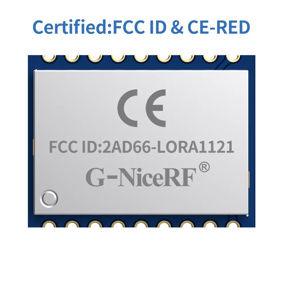
Type: LoRa Front-End Modules
Certification: FCC ID/CE-RED
Size (mm):19.72*15.05
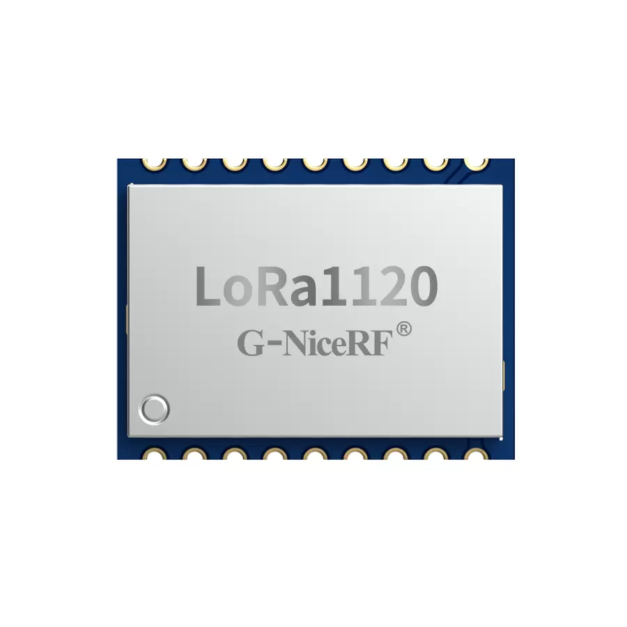
Certification: Others
Modulation: LoRa
Chip: LR1120
Interface: SPI
Output Power: 160mW
Frequency: 433MHz/470MHz/868MHz/915MHz/2.4GHz/1.9GHz
Size (mm):19.72*15

Certification: FCC ID/CE-RED
Modulation: LoRa/GFSK/GMSK/FLRC/4-FSK/O-QPSK
Chip: LR2021
Interface: SPI
Output Power: 160mW
Frequency: 433MHz/470MHz/868MHz/915MHz/2.4GHz/1.9GHz
Size (mm):19.72*15.0
Privacy Policy
· Privacy Policy
There is currently no content available
Email:sales@nicerf.com
Tel:+86-755-23080616